Basic Understanding of Semiconductors
Lgesemi: According to the different electrical conductivity (resistivity) of objects, conductors, insulators, and semiconductors are classified.
1. Conductor: An object that is easily conductive. For example: iron, copper, etc
2. Insulator: An object that is almost non-conductive. For example: rubber, etc
3. Semiconductors: Semiconductors are objects with conductivity properties between conductors and semiconductors. Can conduct electricity under certain conditions. The resistivity of semiconductors is 10-3-109 Ω· cm. Typical semiconductors include silicon (Si), germanium (Ge), and gallium arsenide (GaAs).
Semiconductor characteristics:
1) Under the influence of external energy, the conductivity changes significantly. Photosensitive and thermosensitive components belong to this category.
2) Adding impurities into pure semiconductors significantly increases their conductivity. Diodes and transistors belong to this category.
2.1.2 Intrinsic Semiconductors
1. Intrinsic semiconductor -
a semiconductor with a pure chemical composition. The purity of semiconductor materials used to manufacture semiconductor devices should reach 99.99999999%, commonly known as the "nine 9s". It is in the form of a single crystal in terms of physical structure. The most commonly used in electronic technology are silicon and germanium.
Silicon and germanium are both tetravalent elements, with four outer electrons. The simplified atomic structure model is shown in the following figure:
The outer electrons are minimally bound by the atomic nucleus and become valence electrons. The properties of matter are determined by valence electrons.
The outer electrons are minimally bound by the atomic nucleus and become valence electrons. The properties of matter are determined by valence electrons.
2. Covalent bond structure of intrinsic semiconductors
The atoms in the intrinsic crystal are very close to each other, causing the four valence electrons originally belonging to each atom to be simultaneously attracted by adjacent atoms, forming covalent bonds with the valence electrons of the surrounding four atoms. The valence electrons in covalent bonds are shared by these atoms and bound to them, forming an ordered crystal arrangement in space. As shown in the following figure:
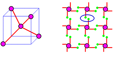 Schematic diagram of spatial arrangement and covalent bond structure of silicon crystals
3. Covalent bonds
The two electrons on a covalent bond are composed of one electron each from adjacent atoms, and these two electrons are called bound electrons. Bound electrons are constrained by two atoms at the same time, and if there is not enough energy, it is difficult to detach from the orbit. Therefore, at an absolute temperature of T=0 ° K (-273 ° C), due to the binding of electrons in covalent bonds, intrinsic semiconductors have no free electrons and are non-conductive. Only under excitation can intrinsic semiconductors conduct electricity
4. Electrons and holes
When a conductor is at a thermodynamic temperature of 0 ° K, there are no free electrons in the conductor. When the temperature rises or is exposed to light, the energy of valence electrons increases, and some valence electrons can break free from the constraints of the atomic nucleus and participate in conduction, becoming free electrons. This phenomenon is called intrinsic excitation, also known as thermal excitation.
At the same time as free electrons are generated, a vacancy appears in their original covalent bond, breaking the atomic electrical neutrality and presenting a positive charge. The positive charge of the vacancy is equal to the negative charge of the electron, and it is commonly referred to as a hole.
Recombination of electrons and holes
The free electrons and holes that appear due to thermal excitation are simultaneously paired, known as electron hole pairs. The free electrons in the free part may also return to the hole, which is called recombination, as shown in the figure. Intrinsic excitation and recombination will reach dynamic equilibrium at a certain temperature.
The movement of voids
Due to the presence of holes in covalent bonds, under the excitation of external energy, adjacent valence electrons may break free and fill the vacancy, and the original position of this electron may become a hole, while other electrons may transfer to that position. In this way, charge transfer - current - occurs in covalent bonds.
The direction of current is opposite to the direction of electron movement and the same as the direction of hole movement. The fundamental reason for the generation of current in intrinsic semiconductors is the presence of holes in covalent bonds. Due to the limited number of holes, its resistivity is very high
The movement of holes in crystals (animation)
2.1.3 Impurity Semiconductor
Introducing certain trace elements as impurities into intrinsic semiconductors can significantly alter their conductivity. The impurities added are mainly trivalent or pentavalent elements. The intrinsic semiconductor doped with impurities is called an impurity semiconductor.
1. N-type semiconductor
Introducing pentavalent impurity elements, such as phosphorus, into intrinsic semiconductors can form N-type semiconductors, also known as electronic semiconductors. Because only four valence electrons in the pentavalent impurity atom can form covalent bonds with valence electrons in the surrounding four semiconductor atoms, and the excess valence electron can easily form a free electron due to the lack of covalent bond binding. In N-type semiconductors, free electrons are the majority carriers, mainly provided by impurity atoms; In addition, silicon crystals generate a small number of electron hole pairs due to thermal excitation, so holes are minority carriers.
In N-type semiconductors, free electrons are the majority carriers, mainly provided by impurity atoms; In addition, silicon crystals generate a small number of electron hole pairs due to thermal excitation, so holes are minority carriers.
N-type semiconductor structure
The pentavalent impurity atom that provides free electrons becomes a positive ion due to its positive charge, so the pentavalent impurity atom is also known as a donor impurity.
So, there are two types of conductive ions in N-type conductors: free electrons - majority carriers (composed of two parts);
Holes - minority carriers
2. P-type semiconductor
Doping trivalent impurity elements such as boron, gallium, indium, etc. into intrinsic semiconductors forms P-type semiconductors, also known as hole type semiconductors.
When trivalent impurity atoms form covalent bonds with silicon atoms, they lack a valence electron and leave a hole in the covalent bond. When electrons on adjacent covalent bonds are excited and gain energy, they may fill the hole and generate new holes. Holes are their main charge carriers.
P-type semiconductor structure
In P-type semiconductors, boron atoms easily become a negative ion with a unit negative charge due to capturing one electron, and trivalent impurities are therefore also known as acceptor impurities. The covalent bond of silicon atoms forms a hole due to the loss of an electron. So the schematic diagram of the structure of P-type semiconductor is shown in the figure.
In P-type semiconductors, holes are the majority carriers, mainly formed by doping; Electrons are minority charge carriers formed by thermal excitation.
3. The Influence of Impurities on Semiconductor Conductivity
Impurities have a significant impact on the conductivity of intrinsic semiconductors, and some typical data are as follows:
At room temperature of T=300 K, the electron and hole concentrations of intrinsic silicon are n=p=1.4 × 10¹⁰/cm з
2. Atomic concentration of intrinsic silicon: 4.96 × 10²²/cm з
3. Free electron concentration in doped N-type semiconductor: n=5 × 10¹⁶/cm з
The above three concentrations basically differ by 1000000/cm з in sequence.