Design Techniques for Electrostatic Protection and ESD Protection Methods
Lgesemi: The theoretical research on electrostatic discharge (ESD) has become quite mature. In order to simulate and analyze electrostatic events, many ESD models have been designed by previous researchers.
Common electrostatic models include human body model (HBM), charged device model, field induction model, field enhancement model, machine model, and capacitive coupling model. Chip level testing is generally conducted using HBM, while electronic products are tested using the discharge model of IEC61000-4-2. In order to standardize the testing of ESD, the European Community's IEC61000-4-2 has established strict transient shock suppression standards in terms of industrial standards. Electronic products must comply with this standard before they can be sold to various member states of the European Community.
Therefore, most manufacturers consider IEC61000-4-2 as the de facto standard for ESD testing. Our national standard (GB/T 17626.2-1998) is equivalent to IEC61000-4-2. Most of the static electricity generators used in laboratories are divided into contact discharge and air discharge according to the IEC61000-4-2 standard. The model of the electrostatic generator is shown in Figure 1. The discharge head is divided into two types: pointed head and round head, according to contact discharge and air discharge.

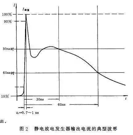
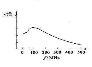
The waveform of electrostatic discharge in IEC61000-4-2 is shown in Figure 2. It can be seen that the main current of electrostatic discharge is a rising edge with a rising edge of about 1ns. To eliminate this rising edge, the response time of the ESD protection device needs to be less than this time. The energy of electrostatic discharge is mainly concentrated in the frequency range of tens of MHz to 500 MHz. Often, we can consider the spectrum, such as using filters to filter out the energy in the corresponding frequency band to achieve electrostatic protection. The discharge spectrum is as follows, which can only be viewed qualitatively and cannot be quantified.
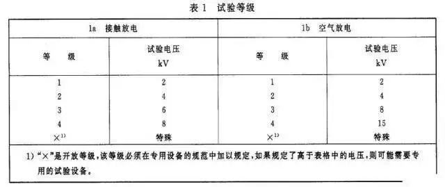
IEC61000-4-2 specifies several test levels, and currently the CTA test for mobile phones is carried out at level 3, which is 6KV for contact discharge and 8KV for air discharge. Many mobile phone manufacturers implement higher levels of electrostatic protection internally.
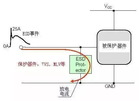
When an integrated circuit (IC) is subjected to electrostatic discharge (ESD), the resistance of the discharge circuit is usually very small and cannot limit the discharge current. For example, when a cable with static electricity is plugged into a circuit interface, the resistance of the discharge circuit is almost zero, causing an instantaneous discharge peak current of up to tens of amperes to flow into the corresponding IC pins. Instantaneous high current can seriously damage ICs, and the heat generated locally can even melt silicon wafer cores. ESD damage to ICs also includes internal metal connections being burnt out, passivation layers being damaged, and transistor cells being burnt out.
ESD can also cause IC deadlock (LATCHUP). This effect is related to the activation of thyristor like structural units inside CMOS devices. High voltage can activate these structures, forming a high current channel, usually from VCC to ground. The deadlock current of serial interface devices can reach up to 1A. The deadlock current will remain until the device is powered off. However, by then, the IC usually had already burned out due to overheating.
Circuit level ESD protection methods
1. Parallel discharge device
Common discharge devices include TVS, Zener diodes, varistors, gas discharge tubes, etc. As shown in the picture:
1.1 Zener diodes (also known as voltage regulators): By utilizing the reverse breakdown characteristics of Zener diodes, ESD sensitive devices can be protected. However, Zener diodes typically have a capacitance of several tens of pF, which can cause signal distortion for high-speed signals (such as 500MHz). Zener diodes also have a good absorption effect on surges on the power supply.
1.2. Transient Voltage Suppressor (TVS): TVS is a solid-state diode specifically designed to prevent ESD transient voltage from damaging sensitive semiconductor devices. Compared with traditional Zener diodes, TVS diodes have a larger P/N junction area. This structural improvement enables TVS to have stronger high-voltage withstand capability, while also reducing the voltage cutoff rate. Therefore, it has a better effect on protecting the safety of low operating voltage circuits in handheld devices.
The transient power and transient current performance of TVS diodes are directly proportional to the junction area. The junction of this diode has a large cross-sectional area, which can handle high transient currents caused by lightning and ESD. TVS also has junction capacitors, typically ranging from 0.3 pF to several tens of pF. TVS has both unipolar and bipolar types, so be careful when using it.
1.3. Multi layer metal oxide structure devices (MLVs): generally referred to as varistors. MLV can also effectively suppress instantaneous high voltage surges. Such devices have a nonlinear voltage current (impedance) relationship, and the cut-off voltage can reach 2-3 times the initial cut-off voltage. This feature is suitable for electrostatic or surge protection of circuits and devices that are less sensitive to voltage, such as power circuits, button inputs, etc. The MLV protection effect is not as good as TVS, and the varistor has a lifespan aging.
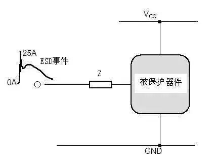
2. Series impedance
Generally, ESD discharge current can be limited by series resistors or magnetic beads to achieve anti-static purposes. As shown in the picture. Ports with high input impedance such as smartphones can be protected by a 1K ohm resistor, such as ADCs, input GPIO, buttons, etc. Don't worry about the 0402 resistor being damaged, it has been proven in practice that it cannot be broken. We won't analyze it in detail here. Using resistors for ESD protection hardly increases costs. If magnetic beads are used, the cost is similar to that of varistors.
3. Add filtering network
As mentioned earlier, the energy spectrum of static electricity can also achieve the purpose of static electricity protection by filtering out the main energy with a filter.
For low-frequency signals such as GPIO input, ADC, and audio input, 1k+1000PF capacitors can be used for electrostatic protection. The cost can be ignored and the performance is not inferior to varistors. If a 1K+50PF varistor (the composite protection measure described below) is used, the effect is better. Experience has shown that this protection effect sometimes exceeds TVS.
For microwave signals of RF antennas, if TVS tubes, pressure-sensitive and other capacitive devices are used for electrostatic protection, the RF signal will be attenuated. Therefore, it is required that the capacitance of TVS be very low, which increases the cost of ESD measures. For microwave signals, a several tens of nH inductor can be connected in parallel to ground to provide a discharge channel for static electricity, which has almost no effect on microwave signals. For mobile phones operating at 900MHz and 1800MHz, a 22nH inductor is often used. This can absorb a lot of energy from the main energy spectrum of static electricity.
4. Composite protection
There is a device called EMI filter, which has excellent ESD protection effect, as shown in the picture. There are also EMI filters based on TVS tubes and varistors. The former is effective but expensive, while the latter is cheap. Generally, the price of 4-channel EMI based on varistors is around 0.02 $.
5. Add absorption circuit
Copper leakage can be added to sensitive signal attachments to absorb static electricity. The principle is the same as that of a lightning rod. Placing pointed discharge points (spark gaps) on signal lines is also commonly used in the design of counterfeit mobile phones.